A transistor is a semiconductor device that amplifies or modifies an electrical signal. Transistors are the building blocks of electronic circuits, such as amplifiers, oscillators, logic gates, and more.
Bipolar junction transistors (BJTs), field-effect transistors (FETs), and metal-oxide-semiconductor field-effect transistors (MOSFETs) are a few examples of the various types of transistors.
In this article, we will learn about one of the most widely used BJTs, the BC547 NPN transistor. We will explain what a BC547 NPN transistor is, its characteristics and specifications, how to use it in various applications, and its pinout and package details.
What is a BC547 NPN transistor?
A BC547 NPN transistor is a small-signal BJT that can be used for general-purpose switching and amplification applications. It has three terminals: collector ©, base (B), and emitter (E). The current flows from the collector to the emitter when a small current is applied to the base.
The amount of current that flows through the collector-emitter path depends on the current gain (hFE) of the transistor, which is typically between 110 and 800 for the BC547.
The BC547 belongs to a family of transistors that share similar characteristics and specifications, such as BC546, BC548, BC549, and BC550.
The main difference between these transistors is their breakdown voltage (VCEO), which ranges from 45 V to 80 V. The BC547 has a VCEO of 45 V, which means it can withstand a maximum voltage of 45 V between the collector and the emitter.
The BC547 also has several subtypes, such as BC547A, BC547B, and BC547C, which differ in their current gain values.
The BC547A has a hFE range of 110 to 220, the BC547B has a hFE range of 200 to 450, and the BC547C has a hFE range of 420 to 800. The higher the hFE value, the higher the amplification factor of the transistor.
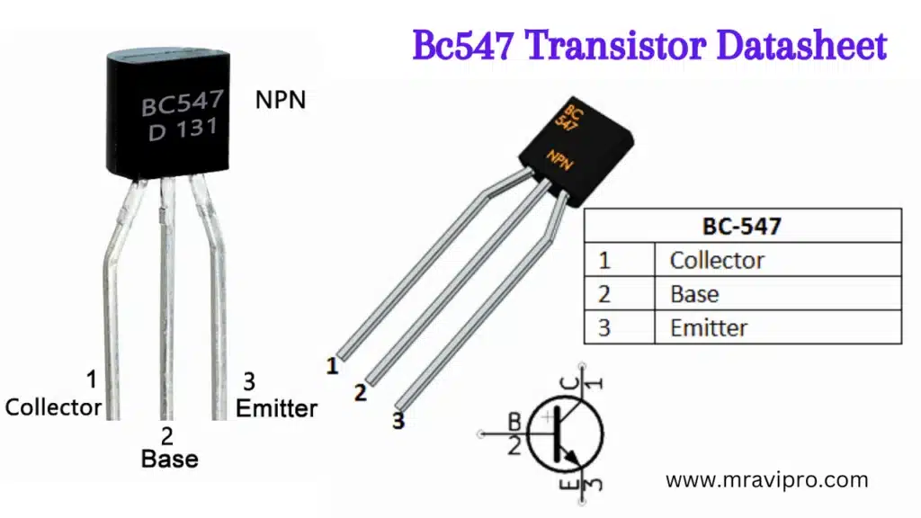
BC547 Pinout
The BC547 pinout is shown in the following diagram:
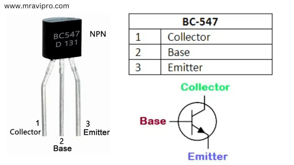
The BC547 pinout has three pins:
- Pin 1: Collector ©
- Pin 2: Base (B)
- Pin 3: Emitter (E)
The BC547 pinout can be identified by looking at the flat side of the transistor, which has the part number printed on it.
The pin that is closest to the left edge of the flat side is the collector pin, followed by the base pin and the emitter pin.
What is the frequency range of BC547?
The frequency range of BC547 is the range of frequencies at which the transistor can operate effectively.
The frequency range depends on several factors, such as the load impedance, the biasing conditions, the temperature, and the circuit configuration.
One of the parameters that indicate the frequency range of BC547 is the transition frequency (fT), which is defined as the frequency at which the current gain drops to unity (hFE = 1).
The fT value for the BC547 is typically around 300 MHz, which means that the transistor can amplify signals up to this frequency.
Another parameter that indicates the frequency range of BC547 is the cutoff frequency (fC), which is defined as the frequency at which the power gain drops to half of its maximum value.
The fC value for the BC547 depends on the circuit configuration and the load impedance. For example, in a common-emitter amplifier with a resistive load of 1 kΩ, the fC value for the BC547 is around 100 kHz.
What is the maximum input and output current of BC547?
The maximum input and output currents of BC547 are the maximum values of current that can flow through the base and collector terminals of the transistor without damaging it.
The maximum input current (IB) is also known as the base current, and the maximum output current (IC) is also known as the collector current.
The maximum input current of BC547 is 5 mA, which means that the base terminal should not receive more than 5 mA of current from an external source.
To limit the base current, a resistor (RB) is usually connected in series with the base terminal. Using Ohm’s law, the value of RB can be calculated:
RB = VBE / IB
where VBE is the base-emitter voltage, which for silicon transistors is approximately 0.7 V.
The maximum output current of BC547 is 100 mA, which means that the collector terminal should not deliver more than 100 mA of current to an external load.
To limit the collector current, a resistor (RC) or another device (such as an LED) is usually connected in series with the collector terminal. RC’s value can be determined using Ohm’s law:
RC = VCC + VCE + IC
Where VCC is the supply voltage and VCE is the collector-emitter voltage, which depends on the operating region of the transistor.
What is the maximum voltage for BC547?
The maximum voltage for BC547 is the maximum value of voltage that can be applied across different transistor terminals without damaging them. The maximum voltage for BC547 is:
- VCEO: The maximum voltage between the collector and the emitter with the base open. For the BC547, this value is 45 V.
- VCBO: The maximum voltage between the collector and the base with the emitter open. For the BC547, this value is 50 V.
- VEBO: The maximum voltage between the emitter and the base with the collector open. For the BC547, this value is 6 V.
Is BC547 an NPN or PNP transistor?
BC547 is an NPN transistor, which means that it has two layers of n-type semiconductor material sandwiching a layer of p-type semiconductor material.
The n-type material has an excess of electrons, while the p-type material has a deficiency of electrons.
The n-type material forms the collector and emitter terminals, while the p-type material forms the base terminal.
The NPN transistor operates using a small current at the base terminal to control a larger current on the collector-emitter path.
When a positive voltage is applied to the base term concerning the emitter terminal, the p-n junction between the base and the emitter becomes forward-biased, allowing a small current to flow from the base to the emitter.
This current creates a depletion region in the base layer, which reduces its resistance and allows a larger current to flow from the collector to the emitter.
The ratio of the collector current to the base current is called the current gain (hFE) of the transistor.
The opposite of an NPN transistor is a PNP transistor, which has two layers of p-type semiconductor material sandwiching a layer of n-type semiconductor material.
The p-type material forms the collector and emitter terminals, while the n-type material forms the base terminal.
The PNP transistor operates using a small current at the base terminal to control a larger current at the emitter-collector path.
When a negative voltage is applied to the base term concerning the emitter terminal, the p-n junction between the base and the emitter becomes forward-biased, allowing a small current to flow from the emitter to the base.
This current creates a depletion region in the base layer, which reduces its resistance and allows a larger current to flow from the emitter to the collector. The ratio of the emitter current to the base current is called the current gain (hFE) of the transistor.
Also, read this article:
- IRFZ44N Mosfet Datasheet: Full Details
- RU6888r Mosfet Datasheet Full Details Download
- How to Make a BLDC Motor ESC Using MOSFET
Conclusion
In this article, we have learned about the BC547 NPN transistor datasheet, including its characteristics, specifications, applications, pinout, and package details.
We have also learned how to use it as a switch or an amplifier in various circuits. We hope that this article has helped you understand more about this versatile and popular transistor.